


!A refers to the negation of variable A, and so on:
R = !A!B + AB
R = !ABC + ABC + A!B!C
Using the above equation, do the following:
- Write it as a truth table
- Simplify it using boolean algebra
- Simplify it using a Karnaugh map
| A | B | C | D | U |
|---|---|---|---|---|
| 0 | 0 | 0 | 0 | |
| 0 | 0 | 0 | 1 | |
| 0 | 0 | 1 | 0 | |
| 0 | 0 | 1 | 1 | |
| 0 | 1 | 0 | 0 | |
| 0 | 1 | 0 | 1 | |
| 0 | 1 | 1 | 0 | |
| 0 | 1 | 1 | 1 | |
| 1 | 0 | 0 | 0 | |
| 1 | 0 | 0 | 1 | |
| 1 | 0 | 1 | 0 | |
| 1 | 0 | 1 | 1 | |
| 1 | 1 | 0 | 0 | |
| 1 | 1 | 0 | 1 | |
| 1 | 1 | 1 | 0 | |
| 1 | 1 | 1 | 1 |
Using the above truth table, write out the following:
- The unoptimized sum-of-products equation, skipping over don't cares
- A Karnaugh map, along with boxes which exploit don't cares where appropriate.
- An optimized sum-of-products equation, derived from the Karnaugh map created in the previous step.
Design a two-bit arithmetic logic unit (ALU) that has the following operations:
ANDthe two operands togetherORthe two operands togetherNANDthe two operands together (that is, AND them and NOT the result)NORthe two operands together (that is, OR them and NOT the result)
Specifically, your ALU will have the following inputs:
| Input Name | Input Description |
|---|---|
A0 |
Bit 0 of the first operand |
A1 |
Bit 1 of the first operand |
B0 |
Bit 0 of the second operand |
B1 |
Bit 1 of the second operand |
S0 |
Select bit 0, used for specifying the operation to perform (see table below) |
S1 |
Select bit 1, used for specifying the operation to perform (see table below) |
Given the above inputs, your ALU will produce the following outputs:
| Output Name | Output Description |
|---|---|
U0 |
Bit 0 of the output |
U1 |
Bit 1 of the output |
As for which operation should be performed, this is based on the values of inputs S0 and S1.
The table below described the values that correspond to the different operations:
Value for S1 |
Value for S0 |
Operation |
|---|---|---|
0 |
0 |
AND |
0 |
1 |
OR |
1 |
0 |
NAND |
1 |
1 |
NOR |
For this task, you may use the following provided components, in unlimited supply:
- AND, OR, and NOT gates
-
4-input multiplexers, which take the following:
- Two selector bits:
S1andS0 - Four operands:
A,B,C, andD
Z. They should be drawn using the symbol below:
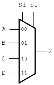
- Two selector bits: