Convert the following Java/C-like code into ARM assembly. The names of the variables reflect which registers must be used for the ARM assembly. Non-register variable names indicate a value that should be stored in memory.
int[] first = new int[]{0, 5, 27, 98};
int[] second = new int[]{1, 2, 8, 29, 42};
int[] result = new int[9];
int r0 = 0;
int r1 = 0;

while (r0 < 4) {
  result[r0] = first[r0];
  r0++;
}

while (r1 < 5) {
  result[r0] = second[r1];
  r0++;
  r1++;
}

for (r2 = 0; r2 < 9; r2++) {
  print_int(result[r2]);
  print_newline();
}
  .equ SWI_Print_Int, 0x6B
  .equ SWI_Exit, 0x11
  .equ SWI_Print_Char, 0x00

  .data
first:
  .word 0, 5, 27, 98
first_length:
  .word 4
second:
  .word 1, 2, 8, 29, 42
second_length:
  .word 5
result:
  .word -1, -1, -1, -1, -1, -1, -1, -1, -1
result_length:
  .word 9

  .text
  .global _start
_start:
  ;; r0: from psuedocode
  ;; r1: from pseudocode
  ;; r2: length of first
  ;; r3: length of second
  ;; r4: first base address
  ;; r5: second base address
  ;; r6: result base address

  mov r0, #0
  mov r1, #0
  ldr r2, =first_length
  ldr r2, [r2]
  ldr r3, =second_length
  ldr r3, [r3]
  ldr r4, =first
  ldr r5, =second
  ldr r6, =result

begin_first_while:
  cmp r0, r2
  bpl end_first_while

  ;; r7: first[r0]
  ldr r7, [r4, r0, LSL #2]
  str r7, [r6, r0, LSL #2]

  add r0, r0, #1
  b begin_first_while

end_first_while:

begin_second_while:
  cmp r1, r3
  bpl end_second_while

  ;; r7: second[r1]
  ldr r7, [r5, r1, LSL #2]
  str r7, [r6, r0, LSL #2]

  add r0, r0, #1
  add r1, r1, #1
  b begin_second_while

end_second_while:

  ;; r7: length of result
  mov r2, #0
  ldr r7, =result_length
  ldr r7, [r7]
begin_for:
  cmp r2, r7
  bpl end_for

  mov r0, #1
  ldr r1, [r6, r2, LSL #2]
  swi SWI_Print_Int

  mov r0, #'\n
  swi SWI_Print_Char

  add r2, r2, #1
  b begin_for

end_for:
  swi SWI_Exit
  .end

An OR gate.

An AND gate.

A NOT gate.
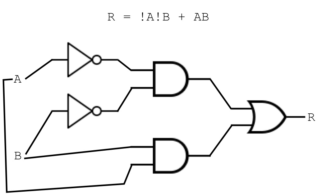
!A refers to the negation of variable A, and so on:
R = !A!B + AB
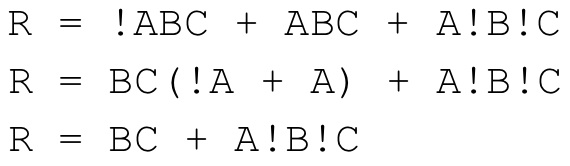
R = !ABC + ABC + A!B!C
Using the above equation, do the following:
- Write it as a truth table:
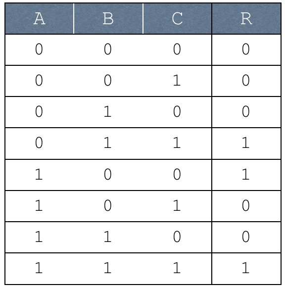
- Simplify it using boolean algebra:
- Simplify it using a Karnaugh map:
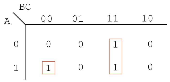
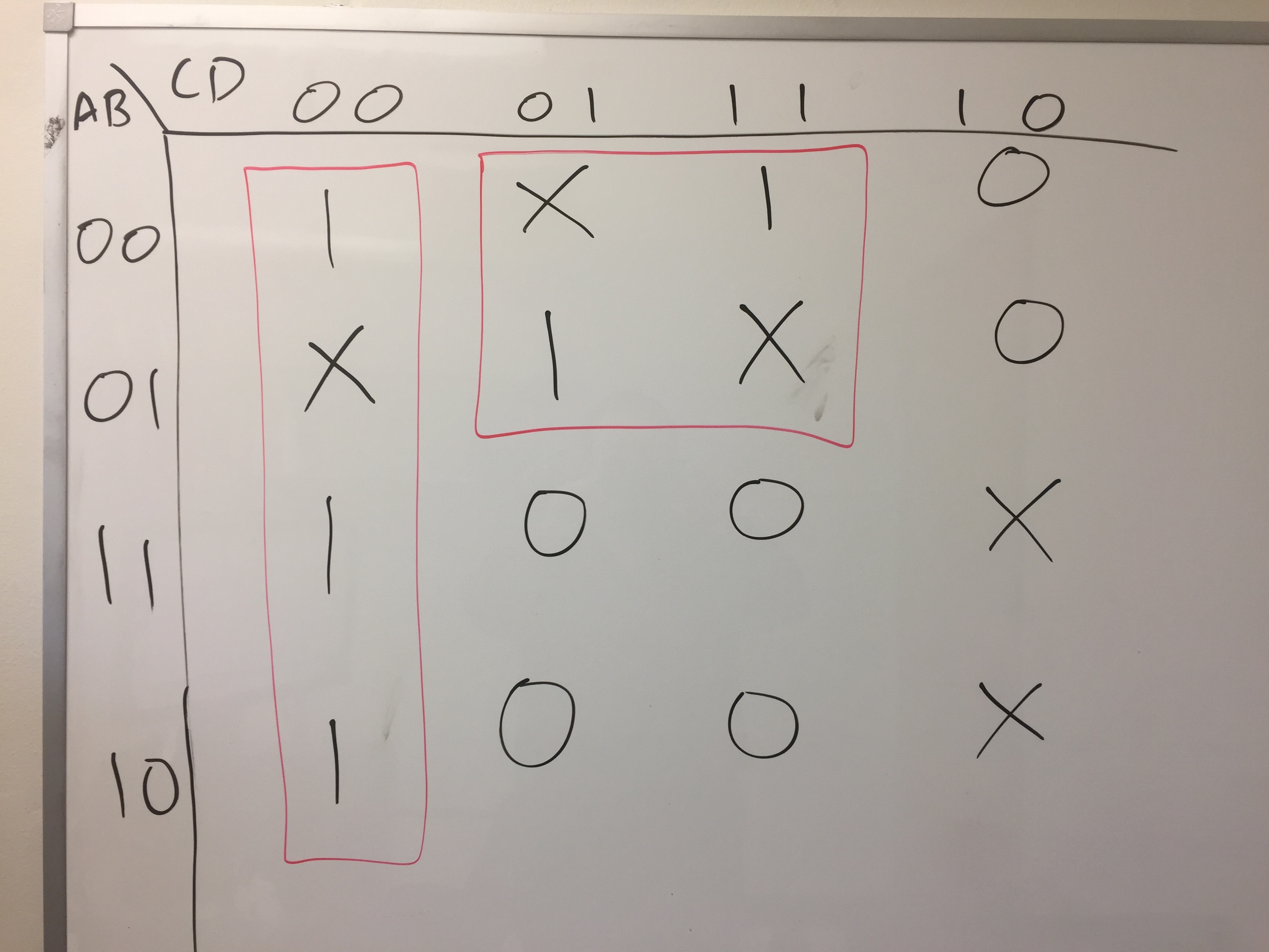
R = A!B!C + BC
| A | B | C | D | U |
|---|---|---|---|---|
| 0 | 0 | 0 | 0 | |
| 0 | 0 | 0 | 1 | |
| 0 | 0 | 1 | 0 | |
| 0 | 0 | 1 | 1 | |
| 0 | 1 | 0 | 0 | |
| 0 | 1 | 0 | 1 | |
| 0 | 1 | 1 | 0 | |
| 0 | 1 | 1 | 1 | |
| 1 | 0 | 0 | 0 | |
| 1 | 0 | 0 | 1 | |
| 1 | 0 | 1 | 0 | |
| 1 | 0 | 1 | 1 | |
| 1 | 1 | 0 | 0 | |
| 1 | 1 | 0 | 1 | |
| 1 | 1 | 1 | 0 | |
| 1 | 1 | 1 | 1 |
Using the above truth table, write out the following:
-
The unoptimized sum-of-products equation, skipping over don't cares
U = !A!B!C!D + !A!BCD + !AB!CD + A!B!C!D + AB!C!D -
A Karnaugh map, along with boxes which exploit don't cares where appropriate.
-
An optimized sum-of-products equation, derived from the Karnaugh map created in the previous step.
U = !C!D + !AD
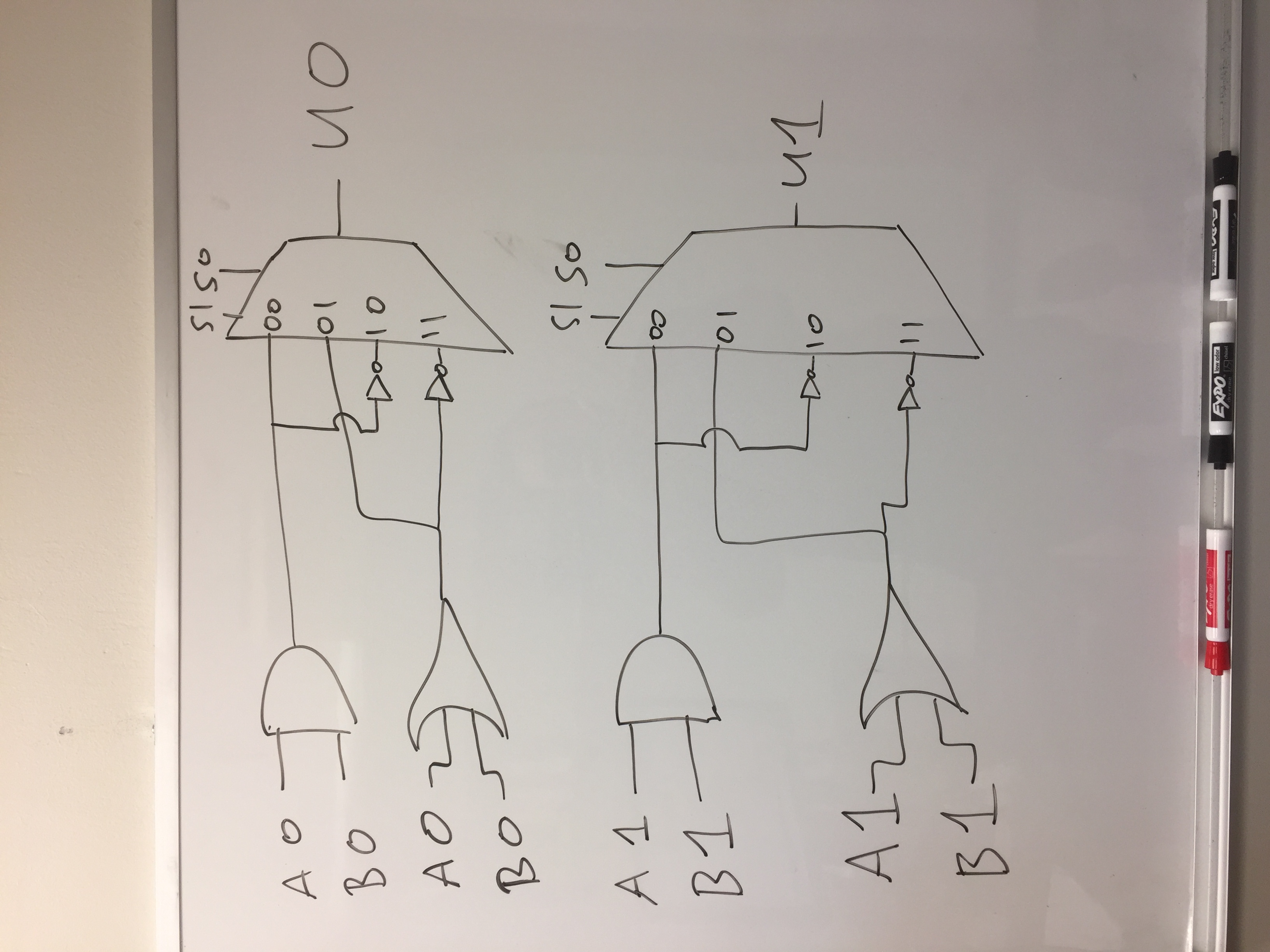
Design a two-bit arithmetic logic unit (ALU) that has the following operations:
ANDthe two operands togetherORthe two operands togetherNANDthe two operands together (that is, AND them and NOT the result)NORthe two operands together (that is, OR them and NOT the result)
Specifically, your ALU will have the following inputs:
| Input Name | Input Description |
|---|---|
A0 |
Bit 0 of the first operand |
A1 |
Bit 1 of the first operand |
B0 |
Bit 0 of the second operand |
B1 |
Bit 1 of the second operand |
S0 |
Select bit 0, used for specifying the operation to perform (see table below) |
S1 |
Select bit 1, used for specifying the operation to perform (see table below) |
Given the above inputs, your ALU will produce the following outputs:
| Output Name | Output Description |
|---|---|
U0 |
Bit 0 of the output |
U1 |
Bit 1 of the output |
As for which operation should be performed, this is based on the values of inputs S0 and S1.
The table below described the values that correspond to the different operations:
Value for S1 |
Value for S0 |
Operation |
|---|---|---|
0 |
0 |
AND |
0 |
1 |
OR |
1 |
0 |
NAND |
1 |
1 |
NOR |
For this task, you may use the following provided components, in unlimited supply:
- AND, OR, and NOT gates
-
4-input multiplexers, which take the following:
- Two selector bits:
S1andS0 - Four operands:
A,B,C, andD
Z. They should be drawn using the symbol below:
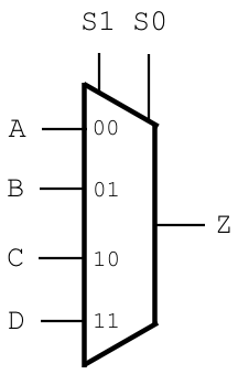
- Two selector bits:
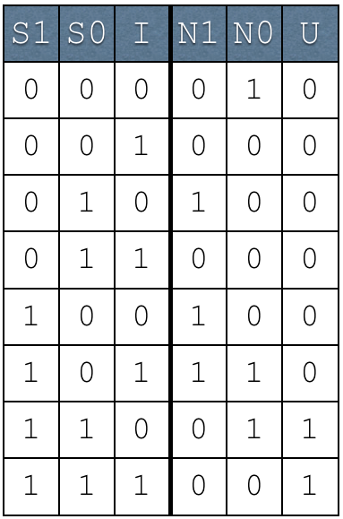
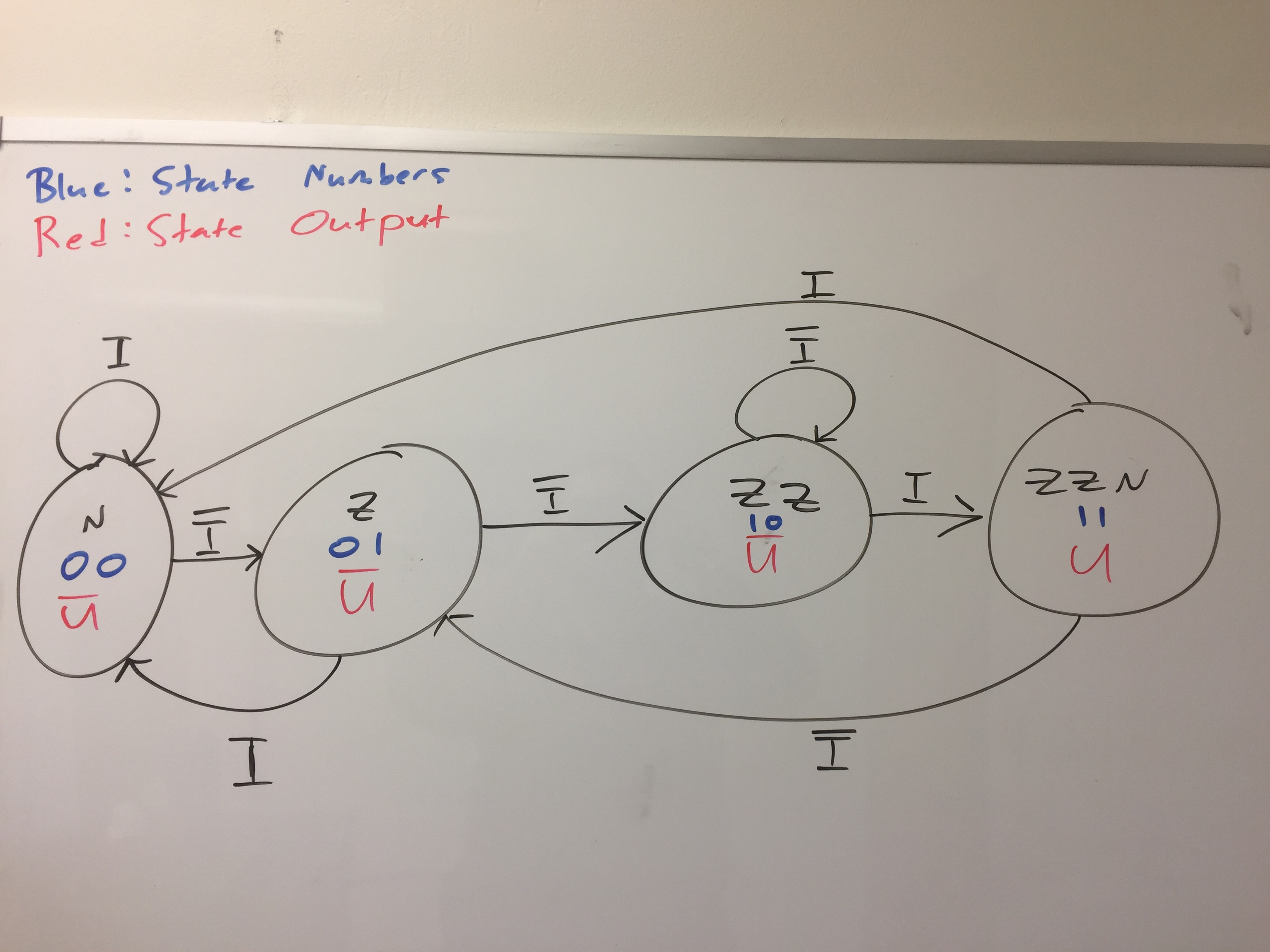
Design a finite state machine (FSM) which will set a particular output U to 1 each time 001 is encountered in a stream of inputs.
Inputs are specified one at a time, and are represented by the variable I.
To illustrate, consider the following example, which shows different values of U and I over time, where each cell is separated by a clock tick:
I |
1 |
1 |
0 |
0 |
1 |
0 |
0 |
1 |
1 |
U |
0 |
0 |
0 |
0 |
0 |
1 |
0 |
0 |
1 |
For this task, you should be able to:
-
Draw the FSM.
-
Define how many latches/flip-flops are necessary to implement your design.
2 (two state bits needed) -
Draw a truth table corresponding to this FSM, taking into account the inputs, outputs, current state, and next state.